ALD 2019 Innovator Awardee
The ALD Innovator award “For Original Work and Leadership in ALD” will be presented on Monday prior to the Plenary Lectures.
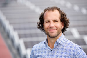
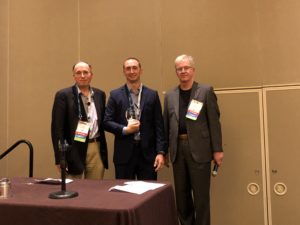
Erwin Kessels, ALD 2019 Innovator Awardee
W.M.M. (Erwin) Kessels
Eindhoven University of Technology TU/e
Biography: Erwin Kessels is a full professor at the Eindhoven University of Technology TU/e where he is also the scientific director of the NanoLab@TU/e clean room facilities. Erwin received his MSc and PhD degree (with highest honors) in Applied Physics from the TU/e in 1996 and 2000, respectively. His research interests cover the field of synthesis of ultrathin films and nanostructures using methods such as (plasma-enhanced) atomic layer deposition (ALD) and atomic layer etching (ALE). Within the field of ALD, he has contributed most prominently by his work on plasma-assisted ALD, his research related to ALD for photovoltaics, and ALD for nanopatterning (including area-selective ALD). Currently Erwin is focusing his research on atomic scale processing, a field which is believed to grow in importance quickly in the next decade for a wide variety of application domains. He was chair of the International Conference on Atomic Layer Deposition in 2008 (Bruges, Belgium) and he frequently (co-)organizes ALD-related workshops. He will serve as chair ALE workshop in 2020. Erwin is active within the American Vacuum Society and has been President of the Netherlands Vacuum Society. He is an associate editor of the Journal of Vacuum Science and Technology. He is also the founder of the blog AtomicLimits.com and of the ALD Academy.
Abstract: Atomic Scale Processing: From Understanding to Innovation
Atomic scale processing is the collective term for processing methods that are currently more and more being explored – and industrially employed – to prepare thin films and nanostructures in a highly controllable way with atomic scale precision. Atomic layer deposition (ALD) and atomic layer etching (ALE) are two prominent examples but also state-of-the-art nanopatterning and area-selective deposition (ASD) approaches can in many cases be regarded as examples of atomic scale processing. In this presentation, I will address several recent and emerging trends in atomic scale processing and discuss how understanding of the underlying mechanisms has contributed to important innovations in the field, either in research or in industry. Application areas to be addressed are especially nanoelectronics and photovoltaics which I will discuss from my own experience and perspective. Topics to be discussed are: (i) the growing importance of plasma ALD, aspects such as conformality and the role (and control) of ions; (ii) the necessity of in situ metrology methods (e.g. in situ spectroscopic ellipsometry) for process monitoring and advanced surface spectroscopy for obtaining more quantitative insight into fundamental parameters; (iii) the use of ALD in nanopatterning and the interest in area-selective ALD including those combinations with intermediate etch steps; and (iv) the need for isotropic and anisotropic ALE, either thermal or plasma-based.


